Product
NEMST-Matrix2008 系列
Atmospheric Plasma Cleaner_Matri
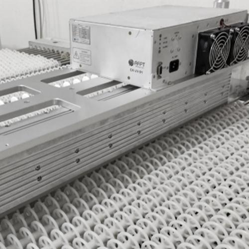
- Dielectric Barrier Discharge (DBD) Plasma Electrodes
- Design With High Plasma Density.
- In-direct/Remote Plasma Design with Single Electrode. (Water Cooling)
- Using N2 for Reaction Gas.
- Electrode width can be designed based on customers' requirements.
- Electrodes can be expanded with higher treatment speed.
- Gap between Electrode and Substrate is about 2 mm.
- Can be Sheet by Sheet or Reel-to-Reel treatment.
- Can be standalone machine or module intregrated with in-line mechanism.
- Single Side Treatment.
- Reaction Gases: N2.
- Gap Between Electrode and Substrate: < 2 mm in general. Plasma Effective Width: 100 mm ~ 2000 mm. (Can be larger based on customers' requirements).
- Treatment Speed: 0.5 ~ 5 m / min in general (Can be changed based on customers' requirements).
- In-direcr/Remote Plasma Design with no ESD.
- Suitable for various materials with sheet or film forms.
- High Plasma Treatment Stability and Uniformity.
- ITO Lead/Finger Cleaning before COG or COF in LCM applications.
- Suitable for Glass/Film Surface Cleaning for Front End or Back End Processes in LCD or OLED Applications.
- Suitable for Glass Cleaning For Cell, Array ,and LCM Applications.
- Surace Cleaning or Modification for Bare Glass or ITO Glass. (e.g. Increase Wettability).
- Surface Cleaning or Surface Modification for Electronics or Non-electronics Devices/Materials. (e.g. PI, PET, PE, Plastic).
- Film Growth Applications.